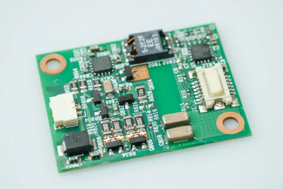
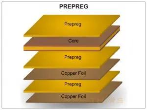
Generally, a standard PCB contains conductive and insulator layers made of core, copper foil, and prepreg materials laminated and compressed together to form an electronic circuit. Depending on the functional intent, PCBs range from simple single-sided boards, made of a core, prepreg, and copper foil, to complex multilayer boards that include many cores, prepregs, and copper foil layers.
The internal layers of a printed circuit board are composed of signal planes, power planes, ground planes, and routing layers. Solder masks and silkscreen layers are the visible layers on a printed circuit board. In single-sided PCBs, electronic components are housed only on the top layer, whereas in multilayer PCBs, electronic components are found on both the top and bottom layers.
Core
A core, also called a substrate or laminate, is a cured, solid, nonconducting material laminated with copper. Traces are placed on the core layer of a PCB.
Copper Foil
Copper foil serves as the conductive layer of a PCB on which the circuit design is printed for further processing. Traces required for the circuit design are left on the PCB, and other copper areas are etched away.
Signal Plane
Signal planes carry electrical signals across components. The design and layout of signal planes involve careful consideration of the impedance offered by each
Power Plane
Power planes carry power supply voltages to different components and circuit sections. They act as a reservoir of power and provide low-impedance paths for the distribution of power throughout the PCB. The power plane establishes a stable voltage supply connecting the PCB to the power line.
Ground Plane
A ground plane, also known as a reference plane, is a dedicated layer in a printed circuit board that provides path for electrical currents to return to the power source. It acts as a stable reference point for voltage levels and serves as a common ground reference for the entire circuit. The ground pin of an electronic component is connected to the ground plane.
Many ground planes are also utilized in certain PCB stackups for electromagnetic shielding and heat dissipation. Electromagnetic shielding is the process of preventing electromagnetic fields from entering or leaving a certain area to ensure that it doesn’t interfere with electronic devices or impact the surrounding environment. Ground and power planes are often used as reference points for signal integrity and to distribute power evenly throughout the board.
Prepreg
A prepreg is a flexible sheet made of a dielectric material. A prepreg serves as an isolation layer between conductive layers in a PCB, such as the core and copper foil. The binding quality of the prepreg material binds the layers together and protects the PCB from the external environment and corrosion.
Routing Layer
A routing layer of a PCB refers to a specific layer dedicated to routing electrical traces that various components and circuit elements on the PCB. Routing layers are sandwiched between other layers of the PCB stackup, such as signal planes, power planes, and ground , or can be found on the top and bottom layers. The primary purpose of a routing layer is to provide a platform for routing signal traces, power connections, and ground connections to establish the desired electrical connections between components the PCB.
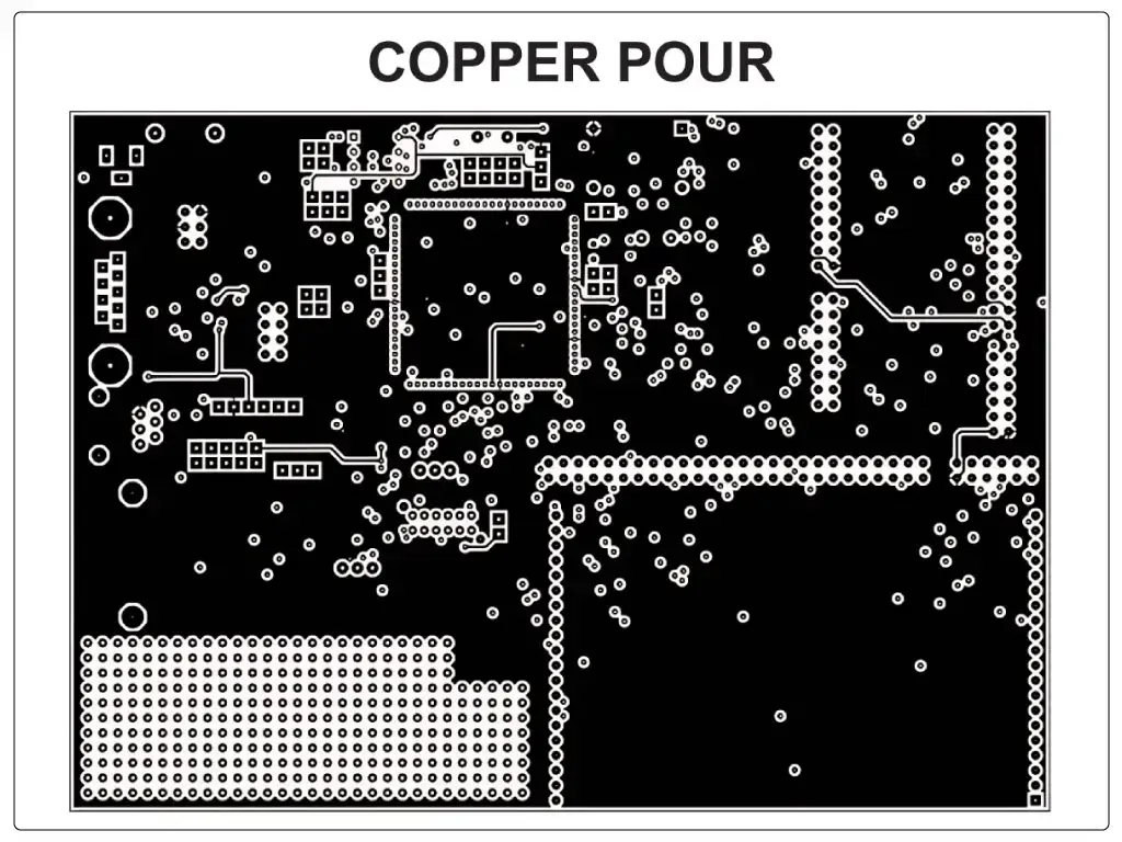
Copper Pour
Copper pour is the copper-filled area on the PCB. Copper pour can be used on the top, bottom, and internal layers of the printed circuit board. However, in simple PCB designs, copper pour may not be necessary.
Copper pour is used to lower the impedance, reduce interference, , and as a heat sink to draw excess heat away from a component. Although copper pour can create physical separation or spacing between components, it does not provide electrical isolation between them. A power plane and a ground plane can also be created with the help of copper pour.
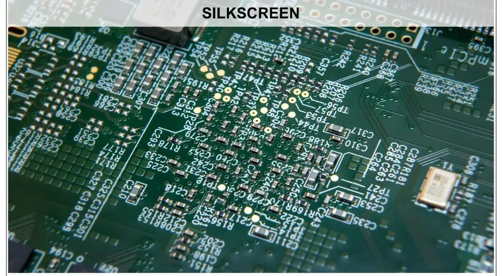
Silkscreen
Silkscreen is the topmost layer of ink markings visible on a PCB that gives details about the components to be mounted on a PCB. Furthermore, warning symbols, testing points, and identification numbers are also marked out on the silkscreen layer. A computer file consisting of the markings is stored for future reference. The legibility of the silkscreen layer is dependent on the size of the PCB. Silkscreen is used, it conveys details about the component location and orientation on a PCB, which is helpful during assembly.
Solder Mask
The solder mask covers all areas except for the PCB pads, which designate the location where each component’s pins, or leads, should be soldered The solder mask helps insulate and protect the copper traces, PCB pads, and other conductive areas on the PCB from short circuits and environmental contaminants.
Are you aware that THORS has launched a new course on PCBs? The THORS Printed Circuit Board (PCB) Basics course is designed to offer learners from various backgrounds a comprehensive understanding of the basic terminology and various technologies associated with PCBs.