Constant research is being done with semiconductor materials that will aid in the development of faster chips, reduce environmental hazards, and cut down the cost of production. Let’s look at the emerging trends in semiconductor materials.
Rebirth of Germanium
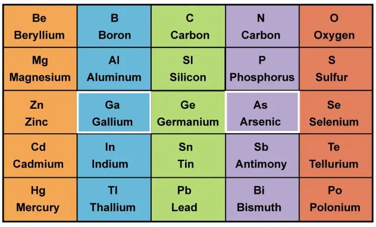
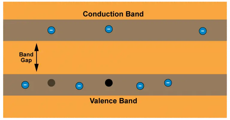
On the periodic table, germanium, gallium, and silicon are all semiconductor materials. Silicon has replaced germanium as the most widely used semiconductor material due to its abundance and thermal conductivity, which enables it to draw excess heat away from the chip. Furthermore, the enables silicon to prevent current leakage in the “off” state. In the “off” state, the charge carriers do not have enough energy to cross the large band gap and reach the conduction band, minimizing leakage current.
Germanium still has a role in the development of a chip. A layer of germanium deposited over silicon has been used to create nanowire devices, which are state of art in transistors. In the future, germanium might return to being the primary semiconductor material. Scientists have found that electron mobility is three times faster and hole mobility is four times faster in germanium than in silicon. This makes germanium an ideal material for Complementary Metal Oxide Semiconductor (CMOS), which employs both n-type transistors and p-type transistors. The enhanced electron and hole mobility provided by germanium aids in making faster transistors that utilize considerably less energy. Manufacturers are contemplating if germanium can potentially make a comeback as a revolutionary material to propel the growth of the semiconductor industry. Incorporating germanium in the channel between the source and drain terminals , devising gate dielectric for germanium, and the other challenges are being researched and focused on in experiments.

Compound Semiconductor Material
Gallium arsenide (GaAs), a group III and group V compound semiconductor material, is composed of the elements gallium (Ga) and arsenic (As). It is a powerful semiconductor compound that can amplify high frequency signals and is used in some high end semiconductor devices. GaAs is widely used in various applications including electronics, optoelectronics, and telecommunications. It offers several advantages over other semiconductor materials, such as silicon, including higher electron mobility and a direct band gap that enables efficient light emission and absorption. GaAs is commonly used in high frequency and high power electronic devices, such as microwave transistors, laser diodes, and solar cells.
Indium-arsenide is another group III and group V compound semiconductor material that has excellent electron mobility compared to germanium and silicon. HoweverThis makes the construction CMOS challenging, as the speed of Positive-channel Metal Oxide Semiconductors (PMOS) becomes lower than the speed of Negative-channel Metal Oxide Semiconductors (NMOS), causing design constraints.
Wide-Band Gap Semiconductors
Wide-band gap semiconductors, such as gallium nitride (GaN) and silicon carbide (SiC), offer advantages like higher breakdown voltage and thermal conductivity, making them ideal for specific applications. High power gallium nitride has the potential to enable more efficient and faster power conversions in electric grid systems. Researchers have found that controlled doping of gallium nitride reduces power loss, which happens during power conversions in power switches. GaN offers superior bandwidth and power density in comparison to alternative technologies, playing a crucial role in the global development and deployment of 5G networks.
Silicon carbide is another material that is gaining popularity in electric vehicles. With a thermal conductivity more than three times higher than silicon, SiC allows for the utilization of smaller die while maintaining the same temperature rise.
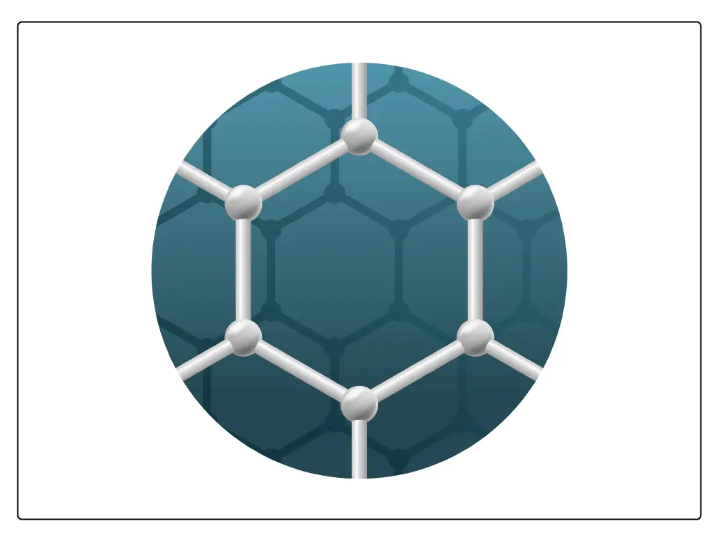
Role of Graphene in Emerging Trends in Semiconductor Materials
One of the prevailing challenges that semiconductor manufacturing industries encounter today is the limitation in reducing the size of logic gates to the microscopic level, while ensuring their ability to withstand the necessary electrical currents for functionality. However, researchers have made a significant discovery: Graphene-based transistor gates can operate with significantly lower energy requirements, enabling them to function at higher speeds without compromising the integrity of the chip. This breakthrough presents the possibility of developing computing devices that are potentially smaller, more stable, and capable of ushering in a new realm of innovation in the field of electronics. Graphene is also assumed to replace tantalum nitride, which is used as a barrier layer in interconnects. However, the chemical and mechanical processes involved in silicon-based semiconductor manufacturing differ significantly from those needed to produce graphene transistors.
All these emerging trends in semiconductor materials are geared towards creating powerful microchips that will power the innovative technology of the future. Are you interested in learning about how a semiconductor is manufactured and the various processes and materials involved in creating powerful microchips? The THORS course, Semiconductor Manufacturing I, will be a great starting point for you.