
Training
Benefits of eLearning in Manufacturing
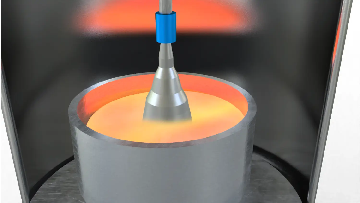
In the world of manufacturing, training is essential. Every employee needs to understand how to use equipment, follow procedures, and maintain quality standards. With the advent

Training
5 Reasons Why a Culture of Learning can Lead to Success
Learning is continuous. After all, there are always new skills to learn and techniques to adopt. A culture of learning in an organization can also
Electronics
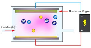
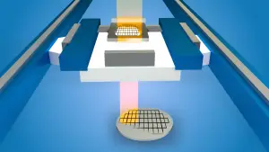
The Evolution of Resistor Technology: From Wire to What’s Next?
Understanding the evolution of resistor technology highlights their crucial role in electronic circuits and how their advancements have shaped modern electronics. It also drives innovation