
Electronics
LEDs and Laser Diodes: A Tale of Two Semiconductor Devices
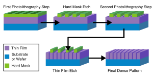
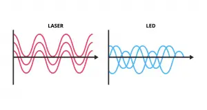
Light Emitting Diodes (LEDs) and laser diodes are two of the most common types of diodes, which are semiconductor devices known for their ability to
Career Planning
Women in Manufacturing: An Interview with Kavita Krishnamurthy
As part of a tribute to women in manufacturing, we at THORS eLearning Solutions decided to showcase one of our own, Kavita Krishnamurthy. Kavita is
Electronics
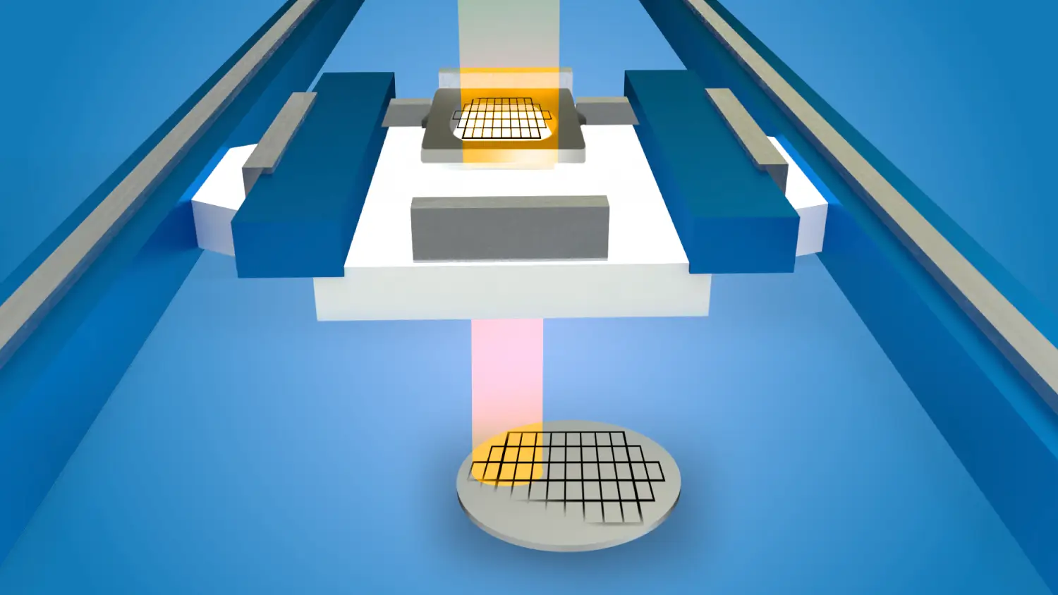
Semiconductor Chip Shortage Significance
In an increasingly interconnected world driven by technological advancements, a looming crisis has captured the attention of industries, governments, and individuals alike: the semiconductor chip