Semiconductors embody the marvel of miniaturization. By shrinking electronic components to microscopic dimensions, semiconductor technology has unlocked a world of possibilities, enabling the creation of increasingly powerful and compact devices. The relentless pursuit of smaller, faster, and more efficient semiconductors underscores the necessity for semiconductor metrology, inspection, and defect detection in semiconductor manufacturing. This focus ensures the highest quality and performance of the devices as they continue to scale down in size.
What is semiconductor metrology and inspection?
Semiconductor metrology involves the measurement and examination of semiconductor materials, devices, and processes to ensure quality, accuracy, and reliability in semiconductor manufacturing. This includes assessing the physical, chemical, and mechanical properties of materials, and monitoring process parameters for control and optimization.
On the other hand, inspection is the process of identifying, characterizing, and reviewing defects on the front surface, back surface, and edge of the wafer that may occur during the semiconductor manufacturing process. The defect location is precisely identified on the wafer for further analysis or correction.
From measuring critical dimensions and material properties to assessing device functionality and reliability, semiconductor metrology and inspection play a crucial role in every stage of semiconductor manufacturing, from research and development to production and quality control.
Why is semiconductor metrology and inspection important?
Semiconductor metrology and inspection holds significant importance for the following reasons:
Understanding the Physical, Chemical, Mechanical, and Electrical Properties of Materials
Semiconductor metrology enables a deep understanding of the physical, chemical, mechanical, and electrical properties of different materials utilized in semiconductor fabrication. For instance, precise measurements of thin film thickness, surface roughness, and material composition aid in optimizing the performance and reliability of semiconductor devices.
Ensuring Process Control to Avoid a Domino Effect
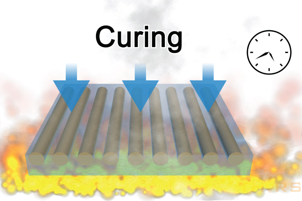
Semiconductor metrology and inspection play a crucial role in process control, allowing manufacturers to monitor and adjust fabrication processes in real time to enhance quality and consistency. Semiconductor manufacturing over a duration of one to two months. Even a minor defect in one step can initiate a chain reaction, impacting subsequent stages. For example, an inaccurate dielectric film thickness could impact the subsequent etching step, altering the overall resistance and capacitance of the device, and potentially affecting its performance.
Defect Detection in Semiconductor Manufacturing
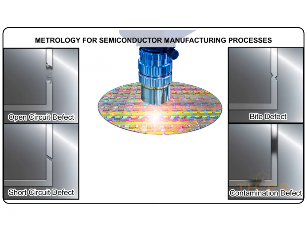
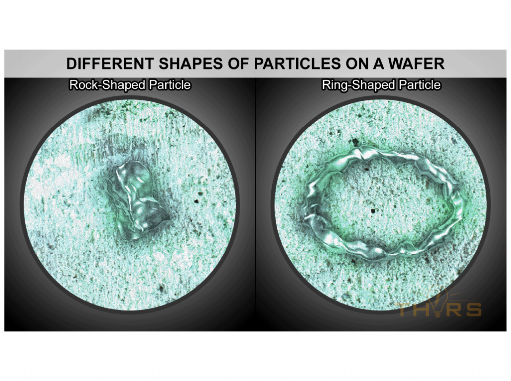
Semiconductor metrology and inspection facilitate the detection of defects and anomalies during various stages of semiconductor production. For example, inappropriate exposure and development time during photolithography can lead to defects in patterned lines, resulting in open circuit defects, short circuit defects, bite defects, and line contamination defects. Advanced imaging techniques such as Scanning Electron Microscopy (SEM) and Atomic Force Microscopy (AFM) enable the identification of defects like particle contamination, pattern irregularities, and material discontinuities. Early detection of defects allows manufacturers to take corrective actions promptly, minimizing scrap and rework.
Increasing Chip Yield
Semiconductor metrology and inspection contribute to increasing chip yield, which is a measure of the number of functioning chips that meet specifications compared to the total number of semiconductor chips fabricated on a wafer. A higher chip yield means that more devices can be produced with the same amount of raw materials, time, and cost. Semiconductor metrology data can identify systematic process issues and variations, enabling process optimization and chip yield enhancement procedures.
Conclusion
By providing invaluable insights into the characteristics and behavior of semiconductor devices, metrology enables semiconductor manufacturers to optimize processes, improve yields, and deliver cutting-edge products that meet the demanding requirements of modern technology-driven markets. Are you interested in learning more about semiconductor metrology? The THORS Semiconductor Metrology Basics course would be a good starting point.