The semiconductor metrology instrument industry has been constantly evolving due to semiconductor miniaturization and the pursuit of higher performance to create more and more powerful logic and memory chips. This progress has pushed the semiconductor metrology instrument industry to adopt new technologies and integrate advanced instruments and techniques, enabling the inspection of increasingly smaller and more powerful chips. This growth trend drives the semiconductor metrology instrument market to expand approximately $10.5 billion by 2030.
Eight key emerging trends and advancements in semiconductor metrology that are shaping the industry are discussed below, in no particular order.
1- Electron Beam Technologies
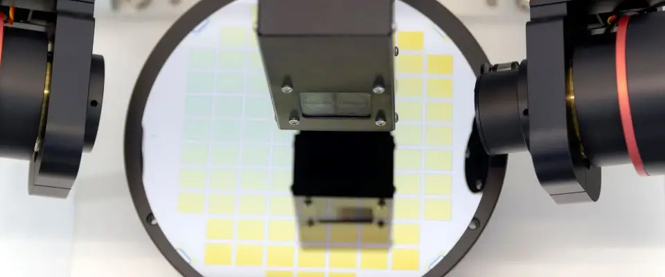
Electron Beam Inspection System detects minute physical defects, reducing the likelihood of chip yield loss and enhancing overall device performance in advanced logic, DRAM, and 3D NAND devices.
Advantage: It is especially useful when optical imaging is inadequate, such as for structures smaller than 10 nm.
Scanning Electron Microscope (SEM) also uses electron beam technology to provide high-resolution measurement of surface morphology, metal film composition, Critical Dimension (CD) etch selectivity, surface roughness, implant and anneal uniformity, and doping concentration.
Advantage: It can produce topographical data and identify defects as small as 1 nm.
2- X-Ray Based Techniques
X-ray based techniques, such as X-ray Photoelectron Spectroscopy (XPS) and X-Ray Diffraction (XRD), are used for nondestructive material characterization, especially thin film thickness, density, and composition analysis.
Advantage: These techniques are particularly useful for buried layers, complex stacks, and high aspect ratio structures that are difficult to analyze with optical methods.
3- Deep Ultraviolet (DUV) Inspection Systems
A DUV inspection system utilizes DUV light, which refers to the shorter-wavelength portion within the UV spectrum, for inspection.
Advantage: DUV inspection finds application in detecting defects as small as a few nanometers, which is not achievable through UV inspection systems or other optical systems. Nodes ranging from 90 nm to 65 nm can be inspected through the DUV inspection system.
4- Extreme Ultraviolet (EUV) Inspection Systems
With the growing adoption of EUV lithography, nondestructive EUV inspection systems are often preferred for monitoring the patterning process in EUV lithography and inspecting reticles.
Advantage : EUV inspection system have higher resolution, reduced masking layers, and simplification of manufacturing.
5- Novel Nanometrology Techniques
Nanometrology techniques, such as spectroscopy with nanoscale resolution, are being created to facilitate the inspection of materials and devices at atomic and molecular scales, offering improved control over the production of miniaturized chips.
Advantage: Novel nanometrology techniques offers precise measurements, detailed characterization, defect detection, and 3D characterization.
6- Artificial Intelligence (AI) and Machine Learning (ML)
AI and ML-driven algorithms are now being integrated into semiconductor metrology instruments to enhance data interpretation, predict wafer defects, improve defect classification, optimize measurement parameters, and improve throughput and yield.
Advantage: This enables more accurate and efficient defect detection, process optimization, and predictive maintenance.
7- Real-time Process Control through In-line Metrology
In-line semiconductor metrology instruments enable wafer inspection during manufacturing, providing real-time process control.
Advantage: This enhances efficiency by allowing quick monitoring and correction at earlier stages, ultimately improving yield.
8- Metrology for Advanced Technology Nodes
Advanced technology nodes, such as Fin Field-Effect Transistor (FinFET), Gate-All-Around (GAA), and 3D NAND, feature 3D structures, buried elements, and complex geometries. Emerging metrology techniques, like Critical Dimension Small-Angle X-ray Scattering (CD-SAXS), which utilizes X-ray diffraction, and enhanced scatterometry for CD measurement of intricate patterns, are becoming increasingly important. Additionally, 3D metrology methods such as confocal sensors, X-ray tomography, and Focused Ion Beam (FIB) tomography.
Advantage: These instruments better enable the 3D visualization of these features.
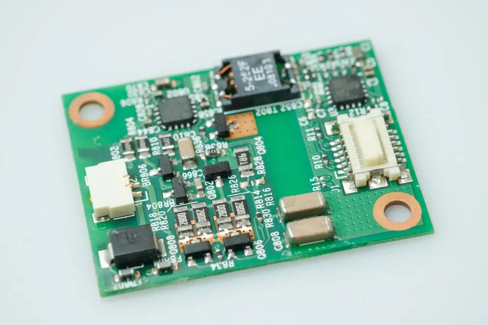
Semiconductor metrology instruments help to identify deviations from design specifications, help to troubleshoot defects, and help optimize manufacturing processes to maximize yield. Therefore, advancements in these instruments are becoming increasingly important and essential for the industry’s progress.
Having this in mind, the THORS Semiconductor Metrology Instruments course introduces learners to the various instruments used in semiconductor testing. This course focuses on wafer inspection systems, which are used for identifying defects, and process control metrology instruments, which are used for measuring various aspects of semiconductor manufacturing processes.
If you are wondering where to begin learning about semiconductor metrology instruments, this course is a great starting point. Click here to view the course introduction video.