

Training
Boosting Employee Engagement in eLearning
Introduction In the realm of modern workplaces, boosting employee engagement in eLearning has become a pivotal factor in fostering productivity, job satisfaction, and overall organizational

Career Planning
How THORS Courses Helped a Mechatronics Student in Germany
Sasshank is an international student attending University in Germany where he studies mechatronics engineering. He was born in Tamil Nadu, where he attended various schools
Electronics
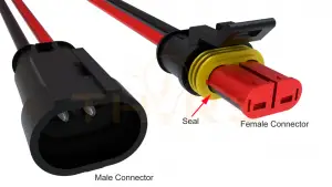
Top 5 Applications of Sealed Connectors in Wiring Harnesses
Sealed connectors in a wiring harness are protective components designed to prevent environmental contaminants such as water, dust, and chemicals from compromising electrical connections. The