Flexible Printed Circuit Boards (PCBs) are expanding the horizons of innovation beyond the limitations of rigid PCBs.
In the past, electronic devices were built by connecting electronic components using wires to form a circuit. The use of wires hampered progress in electronics, as wires were hard to manage. The use of too many wires made electronic components bulky, and circuitries with wires were prone to shorting. The need to address these drawbacks of using wires along with the birth of the Integrated Circuit (IC), spurred the invention of Printed Circuit Boards.
Then, it was found that rigid PCBs were hindering the progress of modern electronics so flexible Printed Circuit Boards were invented, which embraced miniaturization, enhanced efficiency, and promoted adaptability.
Applications of Flexible PCB
Flexible PCBs, unlike traditional rigid PCBs, are made of a flexible plastic material that can be shaped. This paves the way for innovative electronic products in the fields of wearable technology, healthcare, and consumer electronics.
Wearable Technology The lightweight and adaptable flexible PCBs have led to the creation of wearable technology, such as smartwatches, fitness trackers, smart glasses, and air pods.
Healthcare In healthcare, flexible PCBs have aided in the creation of implanters, diagnostic devices, such as CT scans and endoscopic cameras, and advanced sensors for medical monitoring devices, such as blood pressure and heart monitors.
Consumer Electronics Sleek and compact advanced electronics, such as foldable smartphones and portable devices, are putting flexible PCBs at the forefront of innovative electronic designs.
Wearable technology is an example of an application for a flexible Printed Circuit Board (PCB).
How are Flexible Printed Circuit Boards Manufactured?
Manufacturing a flexible PCB follows the same processes as traditional rigid PCB manufacturing but requires different machines, materials, and chemicals.
Process Steps:
Thin copper foil sheets go through drilling, plating, and imaging.
Then, the different layers are aligned and laminated.
Finally, a silkscreen layer is added to the PCB to make it ready for assembly.
Process Step 1: Drilling, Plating, and Imaging
Drilling is the process of creating holes required for the circuit design. The drilling process is performed using high precision drilling machines. Typically, these drilling machines use specialized tools known as drills, or drill bits, to create holes. The type of drill used depends on the size of the hole required for the PCB design.
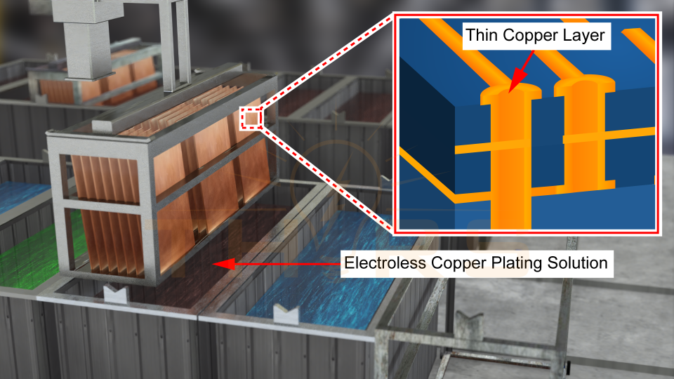
Plating is the process of depositing a thin layer of copper on the walls of the holes and the surface of the conductive areas. Plating is essential for enhancing the conductivity of the drilled holes which improves solderability and prevents oxidation of the copper layer.
The drilled holes in a flexible PCB plated with copper to enable conductivity.
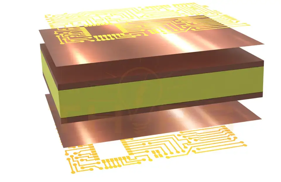
Imaging is the process of transferring circuit patterns by exposing the resist-coated PCB panel to Ultraviolet (UV) light through the photolithography technique. Photolithography is an important process in PCB manufacturing. It involves coating the photoresist on the copper foil layer, exposing the photoresist-coated layer to light from a reticle which holds the circuit pattern, etching the copper areas that are not necessary for the circuit pattern, and then stripping the photoresist off the copper areas.
Circuit patterns printed on the top surface of a single-sided flexible PCB and both the top and bottom surfaces of a double-sided flexible PCB.
Process Step 2: Layer Alignment and Lamination
Similar to traditional PCB layers, a flexible Printed Circuit Board (PCB) also has a few layers. Layer alignment is the process of precisely positioning and arranging the copper foil, adhesives, and polyimide layers.
Lamination is the process of bonding the aligned layers together to form a single sheet.
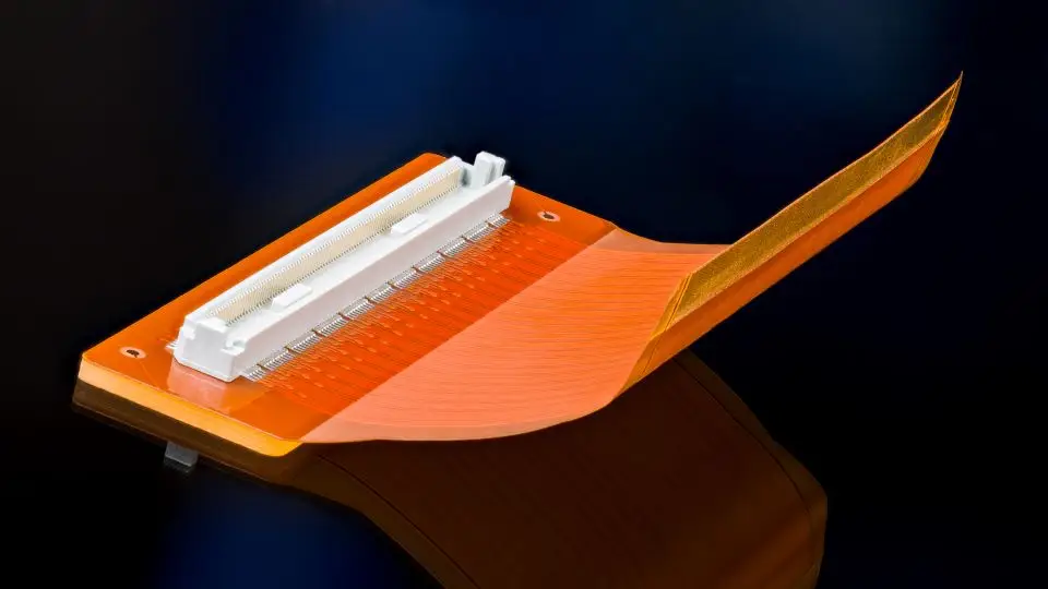
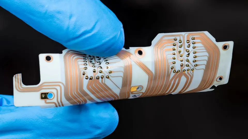
Stiffeners and connectors are added to the laminated flexible PCB before applying silkscreen. Stiffeners are rigid materials, such as polyimide or FR4, applied to certain areas of a flexible PCB to provide additional support where needed. They offer mechanical stability, assist with component mounting, and protect against damage in areas exposed to frequent flexing. Connectors, on the other hand, are components that are designed to link flexible PCBs to other electronics, ensuring secure electrical and mechanical connections.
A stiffener is attached to a portion of a flexible PCB to provide mechanical support.
Process Step 3: A Silkscreen Layer
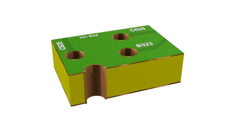
Silkscreen is the topmost layer of ink markings visible on a PCB that gives details about the components to be mounted on a PCB. Furthermore, warning symbols, testing points, and identification numbers are also marked out on the silkscreen. A computer file consisting of the markings is stored for future reference. The legibility of the silkscreen is dependent on the size of the PCB.
Applying the topmost layer of ink markings called the silkscreen to a flexible PCB.
PCBs, in general, have made the once unachievable possible, and flexible PCBs have expanded the boundaries of innovation. By enabling miniaturization, enhancing efficiency, and promoting adaptability, flexible PCBs have become essential in the development of cutting-edge technologies.
Do you want to learn more? The THORS Printed Circuit Board (PCB) Manufacturing course is designed to take you through the processes of PCB manufacturing using engaging and interactive graphics.
Have you ever wondered how your television understands and responds to the commands that are given to the remote control? Breaking apart a television remote…
In an increasingly interconnected world driven by technological advancements, a looming crisis has captured the attention of industries, governments, and individuals alike: the semiconductor chip…